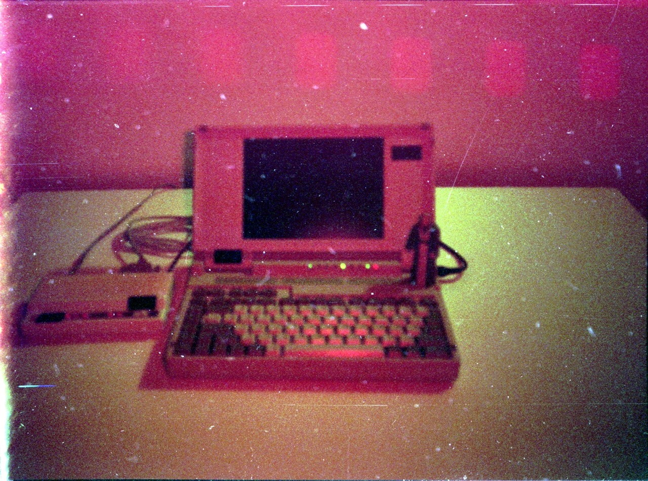
It’s a good candidate since it sounds like there’s no precision mechanical components like there would be in a hard drive. Does anyone have ideas for how I’d go about this? Is there a barrier I’m not considering?
I know how to make basic semiconductors already, so that’s not an issue.
Edit: I’ve got an answer written down in the comments now. TL;DR you’d still need lithography to do it the OG way, because of the patterned magnetic material that directed bubbles around the medium, but material requirements are actually pretty flexible.


Do you understand the physics of the bubble itself at all? I’m a bit unclear on how a this pushes around domain walls in the first place. Like, it makes a kind of sense, electrons hold spin and they’re moving, but the actual physical rate at which they do that is pretty low for even large currents. I take it it’s a magnetic field itself that moves them based on what you wrote? How does that not erase anything?
It does look like two big coils in the diagrams. I wonder if the edge of the wafer was kept “empty” for bubbles to move in and out of, then.
I only vaguely really know what’s going on. I did some more research after commenting, and I think I understand a little bit more. The TI bubble memory has two separate layers. On of them, the ‘magnetic epitaxial film’, basically has a lot of magnetic molecules arranged to point in the same direction. The second layer has circles made of some nickel-iron alloy. What I think is happening is that the actual magnetic bubbles are held on the film, and the iron circles act as tracks the bubbles are pulled along. I don’t think electrons in the bubble are actually moving, but I think the electron spin is. That would explain why the loops are capable of moving the bubbles faster than electrons.
Alright, I guess I should post what I’ve learned.
Soft magnetic (that is, magnetic but not permanently so) thin films will align completely with a magnetic field normal to their surface if it’s strong enough, and of course will lose their magnetisation to thermal fluctuations outside of any field. If the field is intermediate, there’s two possible local states: aligned and anti-aligned, the latter of which is metastable. The thermal fluctuations will cause domain walls to wander naturally at most strengths, although they will have a sort of “surface tension” as the field becomes stronger, since anti-aligned is still the higher-energy state. If the field is just below that necessary to collapse the anti-aligned segments (bubbles) completely, they will be tightly constrained to circles with a diameter on the same order as the film thickness, which are suitable for manipulation.
I imagine to figure out the “collapse field” in a new material, you’d apply a gradually stronger magnetic field to a sample, and look for a discontinuity in instrument readings as the last bubbles collapse. I’d also guess there’s a natural limit here as the thickness of domain walls becomes relevant, so you couldn’t get sub-nm bubbles in an atomic monolayer, but I can’t say for sure. In the 70’s, they were working with films they considered to be 2D, but which are actually pretty thick by 2020s standards.
Bubbles are mobile just as their domain walls are, and slightly repel each other. To move them around, then, a pattern was printed on top of the film in another magnetic material, which would result in bubbles moving one unit one direction if the magnetic field was “wiggled” clockwise, and another if it was “wiggled” counterclockwise. To attract and repel the bubbles in such a way these patterns were asymmetrical, and Intel settled on a sort of chevron. Critically, the coils are much weaker than the permanent magnets in the assembly, so that the bubbles can be moved gently.
To remove bubbles, the field was locally increased with a wire hairpin, and to create a new one the field was weakened somewhat and a pattern was used to split the resulting giant bubble. It’s also possible to use a very strong field in the opposite direction to directly create a bubble, but it was prohibitively energy expensive as a normal operation. I don’t know how exactly the movement of bubbles around the 2D surface was handled, but I honestly bet you could implement a sort of billiard ball logic using the repulsion between bubbles if you wanted, so sky’s the limit.
So, from a DIY perspective the patterning makes this not much better than another kind of solid-state memory, since you’re still doing lithography. What I wonder about, is if you could make a 1D version, either by cutting grooves into a film or by using a thin filament wrapped onto a spool; basically a tape that moves itself in response to a “tilt” relative to the outside field that keeps it written. I have no specific reason to think bubbles would be disrupted by material edges, but there would still be a question about how to protect the bubble-free voids from closing up. I wonder about using more than one layer and exploiting interactions between them; we have a lot more materials to consider now.
Hmm. I’ll keep researching too. Thanks for the help.